Project Description

Features
EPRUI has become the overseas distributor of China’s top gallium nitride (GaN) wafer manufacturer.
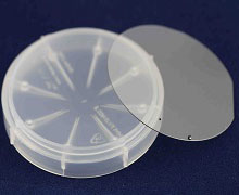
Our freestanding GaN substrate is for UHB-LED and LD. Grown by hydride vapour phase epitaxy (HVPE) technology, Our GaN substrate wafer has low defect density and less or free macro defect density. We can now supply 2 inch,3 inch and 4 inch freestanding gallium nitride wafer for your choice.
2” Freestanding GaN substrate

According to conduction type, there are undoped, Ge doped, semi insulating Fe doped type.
Specification
| Item | GaN50-FS-U | GaN50-FS-N | GaN50-FS-SI |
|---|---|---|---|
| Conduction Type | U-type(Undoped) | N-type(Ge-doped) | Semi Insulating(Fe-doped) |
| Resistivity(300K) | < 0.5 Ω·cm | < 0.05 Ω·cm | >106 Ω·cm |
| Dislocation Density | 1~9x105cm-2 | 5x105 cm-2 | 1~9x105 cm-2 |
| 1~3x106 cm-2 | ~3x106 cm-2 | 1~3x106 cm | |
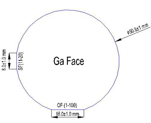
| Dimension | Ф 50.8 mm ± 1 mm | ||
| Thickness | 350 ± 25 µm | ||
| Useable Surface Area | > 90% | ||
| Orientation | C-plane (0001) off angle toward M-Axis 0.35°± 0.15° | ||
| Orientation Flat | (1-100) ± 0.5°, 16.0 ± 1.0 mm | ||
| Secondary Orientation Flat | (11-20) ± 3°, 8.0 ± 1.0 mm | ||
| TTV(Total Thickness Variation) | ≤ 15 µm | ||
| BOW | ≤ 20 µm | ||
| Polishing | Front Surface: Ra < 0.2 nm. Epi-ready polished Back Surface: Fine ground |
||
| Package | Packaged in a class 100 clean room environment, in single wafer containers, under a nitrogen atmosphere | ||
3 inch and 4 inch Freestanding GaN substrate can also be customized.
